The scanning tunneling microscope (STM) was developed at IBM in the 1980s by Gerd Binnig and Heinrich Rohrer, however no introduction to scanning probe microscopy would be complete without mentioning the contribution of Edward Hutchinson (Hutchie) Synge.
E H Synge was the nephew of playwright of John Millington Synge and older brother of physicist John Lighton Synge, and he studied mathematics at (but did not graduate from) Trinity College Dublin. Becoming reclusive after his time at TCD, it was not until after his death that his contributions to what is now known as nanoscience were recognised. In correspondence with Albert Einstein in 1928, Synge elaborated on his idea for a scanning near-field optical microscope (SNOM) capable of optically imaging materials with sub-wavelength resolution by scanning the aperture over the surface, making point-by-point measurements. Unfortunately for Hutchie, his ideas were at least 50 years ahead of their time, with technology only catching up with him after the development of piezoelectric materials to facilitate the scanning mechanism. However, this often-overlooked pioneer described quite succinctly the technology which would later be used for SNOM and STM today.
Imagine attempting to throw a ball to a person on the other side of a wall. Rather than tossing it over the wall, you hurl the ball directly at it, and instead of bouncing off, it passes through to the other side unscathed. This seems fantastic, but this is analogous to the process that occurs on the quantum scale, known as tunneling.
The time-independent Schrödinger equation describes the motion of a particle’s (in this case an electron’s) wavefunction ψn(z) moving under the influence of a potential U(z). For simplicity, the one-dimensional case is considered:
|
| (2.10) |
where ℏ is the reduced Planck’s constant, m is the mass of the electron, E is its energy and z its position.
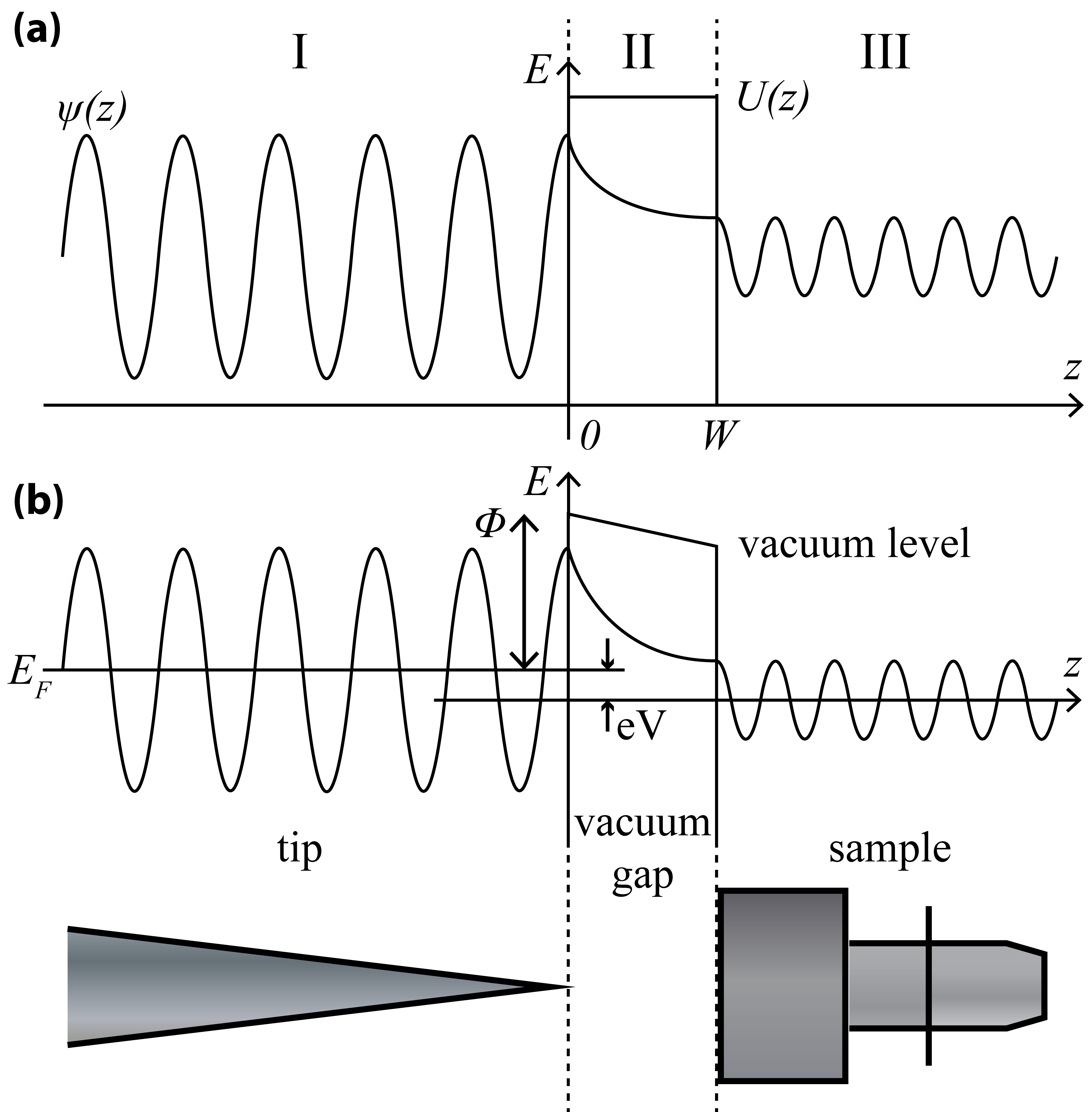
For a wave encountering the potential barrier U(z), as in Figure 2.7a, there are three regimes to consider: (I) the travelling wave before meeting the barrier, where U(z < 0) = 0; (II) the wave inside the barrier, where U(0 < z < W) = U > E; and (III) the wave after encountering the barrier, where U(z > W) = 0. In the classical case, the wavefunction’s value in regimes (II) and (III) would be equal to zero, however when one solves the Schrödinger equation, two solutions are possible; a travelling wave where U(z) < E (regimes (I) and (III)) and an exponential decay within the barrier (regime (II)). We are only concerned with the latter of the two, as this is what governs tunneling.
 | (2.11) |
Since the probability density is given by the square of the wave function and, assuming there is a small bias V between the tip and sample, in order for tunneling to occur there must be a finite probability of finding an electron from z = 0 at z = W, thus:
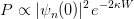 | (2.12) |
If the bias is small, U(z) − E ≈ ϕM, the work function of the sample. ϕM gives the minimum energy needed to bring electrons from the highest occupied energy level (Fermi level, EF , in metals at T = 0 K) to the vacuum level. The small bias also means that only electron states within eV of EF are excited, thus tunneling is mainly by electrons near the Fermi Energy.
However, in order for tunneling to occur (assuming electrons are tunneling from tip to surface, as in Figure 2.7b) there must be empty states of the same energy in the surface for the electrons to tunnel into, therefore the tunneling current is dependent on the density of states, as well as the number of electrons between EF − eV and EF .
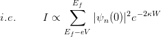 | (2.13) |
By definition, summing the probability over an energy range, such as between EF −ε and EF , gives the number of states available in this energy range per unit volume, i.e. the local density of states, ρs(z,E):
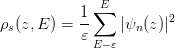 | (2.14) |
Therefore the tunneling current is proportional to the local density of states and a scaling factor which decays exponentially with the width of the gap,
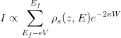 | (2.15) |
An elegant demonstration of the power of the exponential dependence arises when considering typical physical parameters. Taking a value for the work function of ϕM∼4 eV gives κ ≈ 1.025Å−1. If the difference between the distance from the sample of the closest tip atom, d1, and the second closest atom, d2, is d2 −d1 ≈ 1Å , then the ratio between the current flowing through atom 1 to that flowing through atom 2 is I1∕I2 ≈ 10, i.e. a tip atom only 1 Å closer to the surface collects 90% of the current flowing between the surface and tip [54].
It is this exponential dependence of the tunneling current on the gap width which gives the STM its high resolution: in the horizontal plane only those atoms closest to the apex contribute significantly to tunneling; and in the vertical direction, a small 1 Å difference in height changes the current by 10 fold.
Binnig and Rohrer were awarded the 1986 Nobel prize in Physics for their invention of the scanning tunneling microscope (STM). The STM utilises the phenomenon of quantum tunneling in order to visualise the electronic and topological structure of the surfaces of metals and semiconductors. The apparatus consists of an extremely sharp needle or “tip”, the apex of which has a radius of curvature on the order of several nanometers, and is capable of precise positioning and movement. This tip is brought extremely close to the conducting sample, upon which a voltage bias is placed, and the tip is rastered across the sample, recording the tunneling current at every point in the raster scan.
The positioning apparatus usually makes use of the reverse piezoelectric effect. When a voltage is placed across a piezoelectric crystal it undergoes a deformation proportional to the voltage. This deformation is extremely controllable and repeatable, allowing the tip to be positioned with sub-nanometer precision.
The STM can be operated in two modes: constant-current and constant-height. The difference between these modes is illustrated in Figure 2.8. In the constant-current mode, the tunneling current is kept constant using an electronic feedback loop, and the height is varied, thus causing the tip to map out a convolution of the density of states and the topography of the surface. The constant-height mode on the other hand scans the tip at a constant height and records the varying tunneling current due to the corrugation and make-up of the surface.
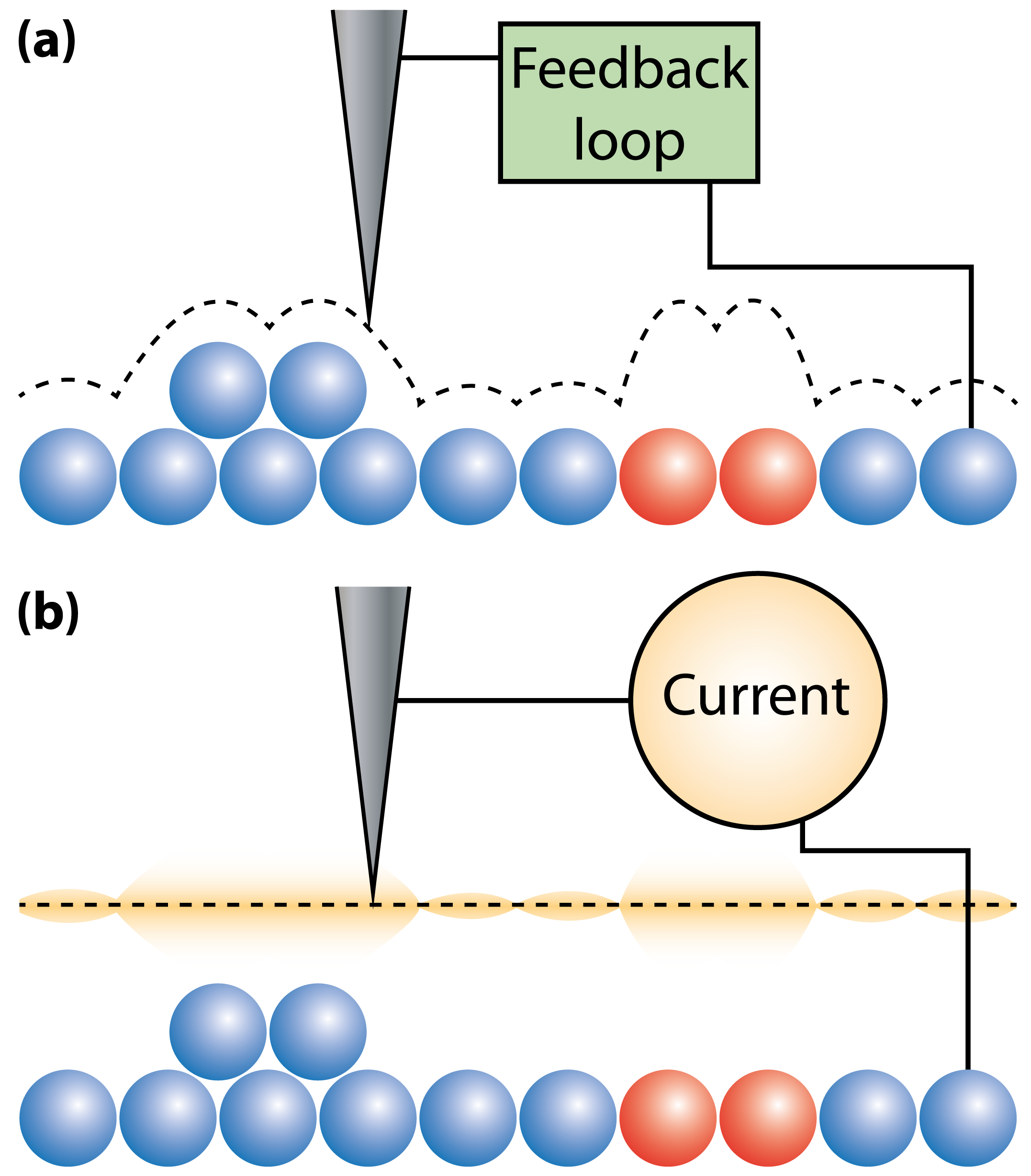
The latter of these two modes is considerably more “risky”, since the roughness of the surface on the nanoscale is unknown before scanning, and so it is inevitable that the tip will come into contact with parts of the surface, either changing the tip’s structure and hence the scanned image, or ruining the tip altogether. The advantage of constant-height over constant-current is that very high speed scanning is possible, since the constant-current mode is limited by the response of the feedback system, however it is only suitable for atomically-flat systems, and so all images presented in this thesis were obtained in constant-current mode.
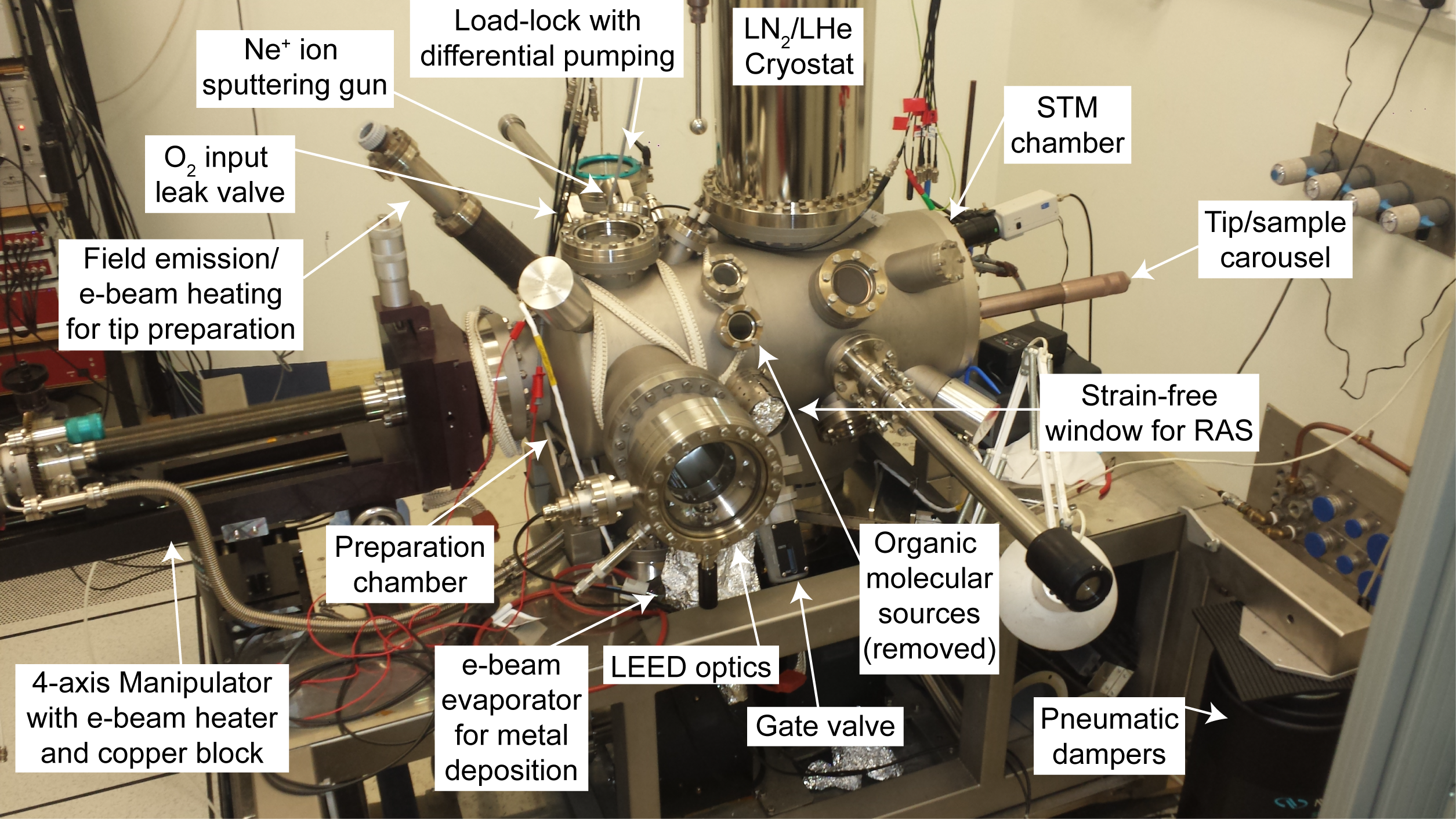
The low-temperature STM (LT-STM) used in Chapters 3 and 5 for the C60 and MnClTPP work is a commercial instrument from Createc GmbH, shown in Figure 2.9, modified to accept “Omicron-style” sample plates. It consists of independent analysis and preparation chambers, separated by a gate valve and each pumped by their own ionisation pump, and a differentially pumped load-lock with a turbomolecular pump. The preparation chamber has a 4-axis (x, y, z and θ) manipulator with integrated electron-beam heater for sample preparation and copper block for LEED measurements and deposition, with optional LN2 cooling.
Also integrated into the preparation chamber are a Ne+ ion sputtering gun, metallic and organic deposition sources, LEED optics, leak valve for gas input and a tip preparation stage with field emission via a single-crystalline Mo plate, and e-beam heating using a “V”-shape filament.
The analysis chamber houses a tip/sample carousel and the STM head. The scanning head is cooled via a two-chamber cryostat compatible with either liquid nitrogen or liquid helium. The head used for measurements in this work was a Besocke-style design, however it has since been replaced by a Slider-type head (commissioning in progress). The tip is magnetically mounted onto the scanning head in both designs, however the Slider scanner allows up to 10 mm of movement in the z-direction, while the Besocke only permitted 2–3 mm of vertical motion.
The entire chamber can be supported by four pneumatic dampers to mechanically decouple it from its environment and reduce noise during scanning.
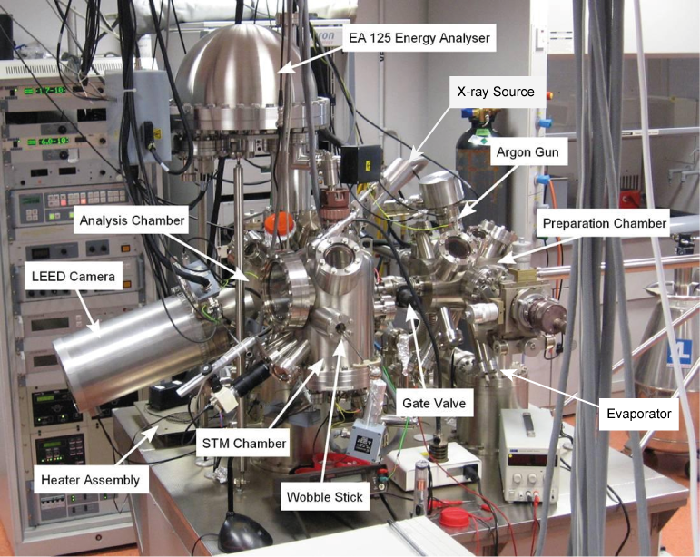
The images of NiDPP in Chapter 4 were obtained using a variable-temperature scanner (VT-STM) from Omicron, shown in Figure 2.10 [55]. Similar to the Createc system, it consists of separate preparation and analysis chambers, and a fast entry load-lock, again with an ionisation pump on each of the main chambers and a turbomolecular pump attached to the load-lock.
The preparation chamber is equipped with an Ar+ ion sputter gun, a manipulator with resistive sample heating and three molecular evaporators. The analysis chamber houses another manipulator with direct and resistive heating, a DAR 400 twin-anode X-ray source, an EA 125 energy analyser for XPS, Omicron LEED optics and the Omicron VT-STM head. In the VT-STM, the sample is placed above the tip with the surface facing down and the tip facing up, in contrast to the Createc scanner.
Data collected by an STM is in the form of an (X,Y,Z) map of height values, i.e. for each of 512 × 512 points in the X–Y plane, the STM records the height of the tip (Z). This is then represented by specialised software [56] as a topographic image. Usually this image will include mechanical noise from the environment, artefacts introduced by tip instability, piezo creep, etc. In order to remove these artefacts, the image is processed by various techniques such as plane subtraction, flattening, smoothing, reducing the Z-range, 2-D fast Fourier transform filtering, drift correction, etc. Some treatments are more radical than others. In this thesis all original STM images have been processed to some degree, the minimum being plane subtraction and Z-range equalisation to enhance contrast, which is applied to all images, however none have been corrected for thermal drift or piezo creep. Any further processing is noted in the relevant figure caption.