2.2 Low-energy electron diffraction
Low-energy electron diffraction (LEED) is based on the diffraction of electrons by
the Bragg planes of a single-crystalline sample. Due to the electrons’ low energy
(typically 10–200 eV), their mean free path in the material is limited to the first
few atomic layers, and so LEED gives information only on the surface’s
topological structure.
The diffraction of electrons by a crystal’s lattice was first observed
experimentally by Davisson and Germer in 1927 [53]. The experiment
was originally intended to study the surface of a nickel target, with the
hypothesis that even the smoothest surface would be too rough for specular
reflection, and would instead diffuse an incident electron beam. However,
after the accidental oxidation of the target, the sample was cleaned in a
high-temperature oven, thus creating single crystallites on the surface.
When the experiment was repeated, they observed that the electrons
were scattered as if by a diffraction grating, and using Bragg’s law it was
shown that the electrons were diffracting from the nickel crystal planes.
This serendipitous result bears mentioning because not only is it the first
experimental evidence of the wave–particle duality of matter, but was also
important for the development of quantum mechanics and the Schrödinger
equation.
2.2.1 Bragg’s law
The diffraction of X-rays from crystalline solids was explained by William
Lawrence Bragg by describing the solid as a series of parallel planes, and the
characteristic spots observed originating from points of constructive interference
of the X-rays. A similar treatment can be performed for electron diffraction, since
the electrons’ de Broglie wavelength is comparable to the interatomic spacing,
however an alternate theory is described in Section 2.2.3 for scattering due to a
surface.
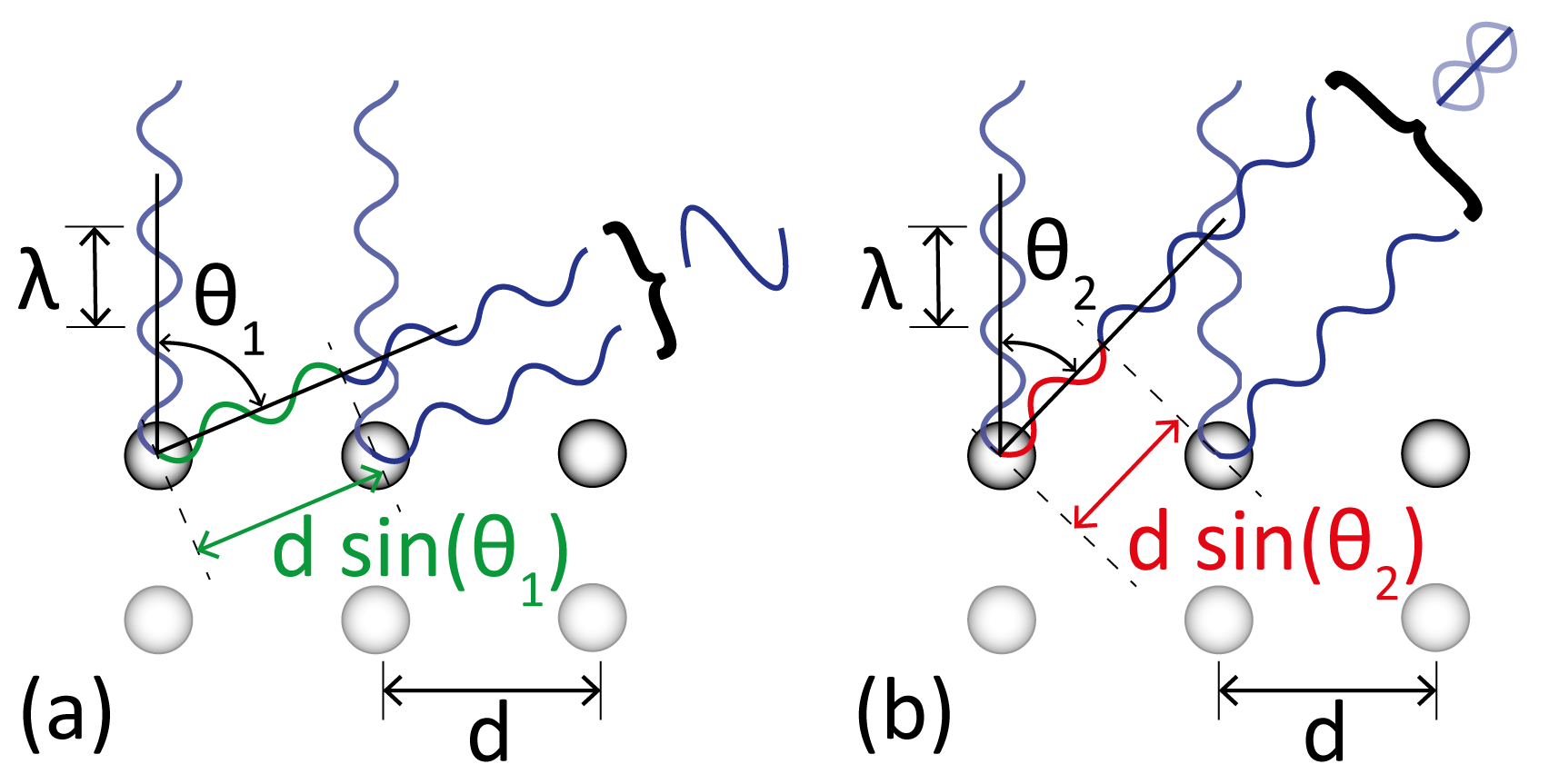
As shown in Figure 2.4, depending on the angle of diffraction from the atoms
in the crystal, the path length difference between the scattered waves reflecting
from different layers of the crystal can cause them to interfere constructively
(Figure 2.4a) or destructively (Figure 2.4b).
The path difference is given by d sin(θ), where d is the interlayer spacing, and
θ is the angle subtended between the incident and diffracted waves. In the case of
Figure 2.4a, the path length difference between the two reflected waves is an
integer number of wavelengths (2λ). This is equivalent to a phase shift of 2π, and
so the two waves constructively interfere. In contrast, in Figure 2.4b the path
difference is equal to one and a half wavelengths, i.e. a phase shift of π, leading to
destructive interference.
The relation derived by Bragg for constructive interference between two waves
at normal incidence was:
 | (2.1) |
where n is an integer and λ is the wavelength of the incident wave.
It is clear from Equation 2.1 that some angles will lead to maxima in the
diffracted beam intensity, but it should be noted that in the case of the diagram,
if only two atoms are involved, there will be a smooth transition between maxima
and minima. In practice, the size of the electron beam in LEED means that many
atoms diffract the beam, mainly sharp peaks are observed, surrounded by
areas of destructive interference. For this reason LEED is an averaging
technique.
Bragg diffraction (and hence LEED) does not directly measure real-space
atomic distances. Instead, the distance between diffraction spots is inversely
proportional to the interatomic spacing, d, and the nλ term is related to the
number of wavelengths that fit between atoms. Therefore, a LEED pattern
describes reciprocal space.
2.2.2 The reciprocal lattice
Reciprocal space effectively represents the periodicity of a Bravais lattice. This is
equivalent to performing a Fourier transform on a periodic function.
Consider a vector  , which represents the Bravais lattice, and a plane wave
ei
, which represents the Bravais lattice, and a plane wave
ei ⋅
⋅ = cos(
 ⋅
⋅ ) + i sin(
 ⋅
⋅ ) which has the same periodicity as the Bravais
lattice.
) which has the same periodicity as the Bravais
lattice.
If their periodicities are equal, then for any point  :
:
The set of vectors  which satisfy the above relation describes the reciprocal
lattice. It is also noted that the reciprocal lattice is itself a Bravais lattice,
and the reciprocal of the reciprocal lattice returns the original real-space
lattice.
which satisfy the above relation describes the reciprocal
lattice. It is also noted that the reciprocal lattice is itself a Bravais lattice,
and the reciprocal of the reciprocal lattice returns the original real-space
lattice.
For an infinite 3-dimensional lattice, defined by its primitive vectors ( ,
, ,
, ),
the reciprocal lattice (
),
the reciprocal lattice ( ,
, ,
, ) is defined as:
 |
(2.2)
(2.3)
(2.4)
|
2.2.3 Surface diffraction
The de Broglie wavelength of an electron, λe is given by:
![∘ -------
---h---- -1.5---
λ = √2meE---; λe[nm ] ≈ Ee[eV]](thesis37x.png) | (2.5) |
where me and Ee are the electron’s mass and kinetic energy, respectively.
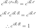
Consider a beam of electrons impinging on a 3-dimensional crystal, as in
Section 2.2.1. For an incident electron with wave vector  = 2π∕hλ0, and a
scattered wave vector
= 2π∕hλ0, and a
scattered wave vector  = 2π∕hλ, the von Laue condition for constructive
interference states that:
= 2π∕hλ, the von Laue condition for constructive
interference states that:
 |
(2.6)
|
i.e.  hkl is a vector
of the reciprocal lattice.
hkl is a vector
of the reciprocal lattice.
Only elastic scattering is considered, and so energy is conserved, i.e. | | = |
| = | |.
As mentioned, the mean free path of electrons within a crystal is small and so
only the first few atomic layers play a role in the diffraction. Therefore, there are
no diffraction elements perpendicular to the surface, and the lattice can be
considered as a 2-dimensional series of rods extending from the surface lattice
points.
|.
As mentioned, the mean free path of electrons within a crystal is small and so
only the first few atomic layers play a role in the diffraction. Therefore, there are
no diffraction elements perpendicular to the surface, and the lattice can be
considered as a 2-dimensional series of rods extending from the surface lattice
points.
Following from this, the 2-dimensional simplification of Equation 2.6 and the
reciprocal lattice vectors become
 |
(2.7)
(2.8)
(2.9)
|
where  is the surface normal unit vector.
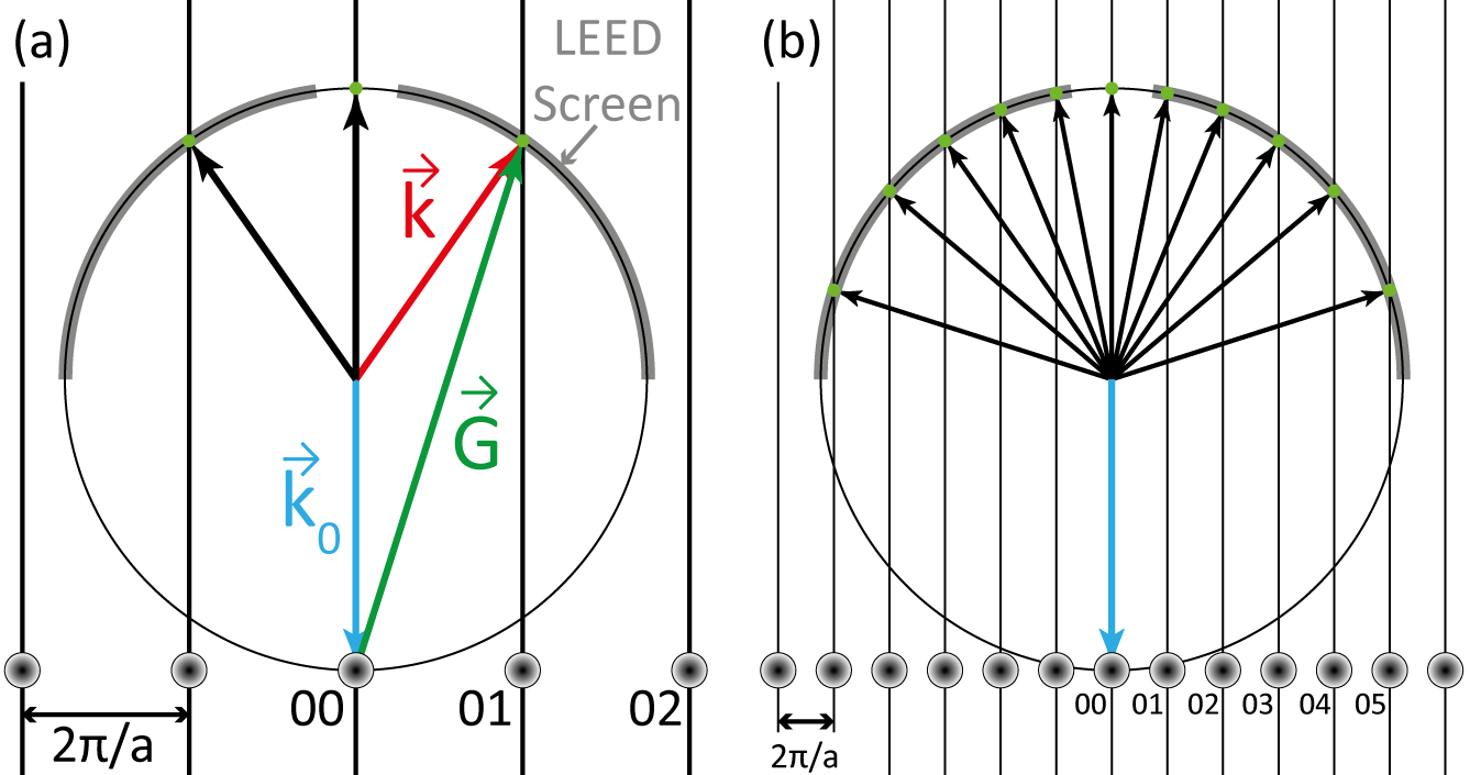
A useful visualisation of the effect of Equation 2.7 is the Ewald sphere, shown
in Figure 2.5.
The Ewald sphere illustrates the points of constructive interference formed by
the incident and diffracted electron waves. The upper half of the sphere can be
considered as the hemispherical fluorescent screen of the LEED apparatus, and
from Figure 2.5b it is clear how a higher kinetic energy leads to more LEED spots
visible on the screen.
2.2.4 Low-energy electron diffraction apparatus
The set-up for LEED is shown in Figure 2.6a.
Electrons are emitted from the electron gun by an accelerating voltage V , and
are diffracted by the sample. They then pass through a series of up to four grids
before colliding with a fluorescent coating on the screen, where light is emitted.
The first and last grids are held at the ground potential to confine the field. The
central grids are kept close to V at V ± δV , in order to select only elastically
scattered electrons. Finally, the electrons are post-accelerated by a high
voltage placed on the screen, in order to maximise the efficiency of the
fluorescence.
A LEED pattern obtained from the clean Mo(110) surface is shown in
Figure 2.6b, showing the hexagonal reciprocal lattice representative of the
close-packed (110) surface of a body-centred cubic crystal.

 lies parallel to the vertical
00 rod. The spots (rods) are numbered by their
lies parallel to the vertical
00 rod. The spots (rods) are numbered by their 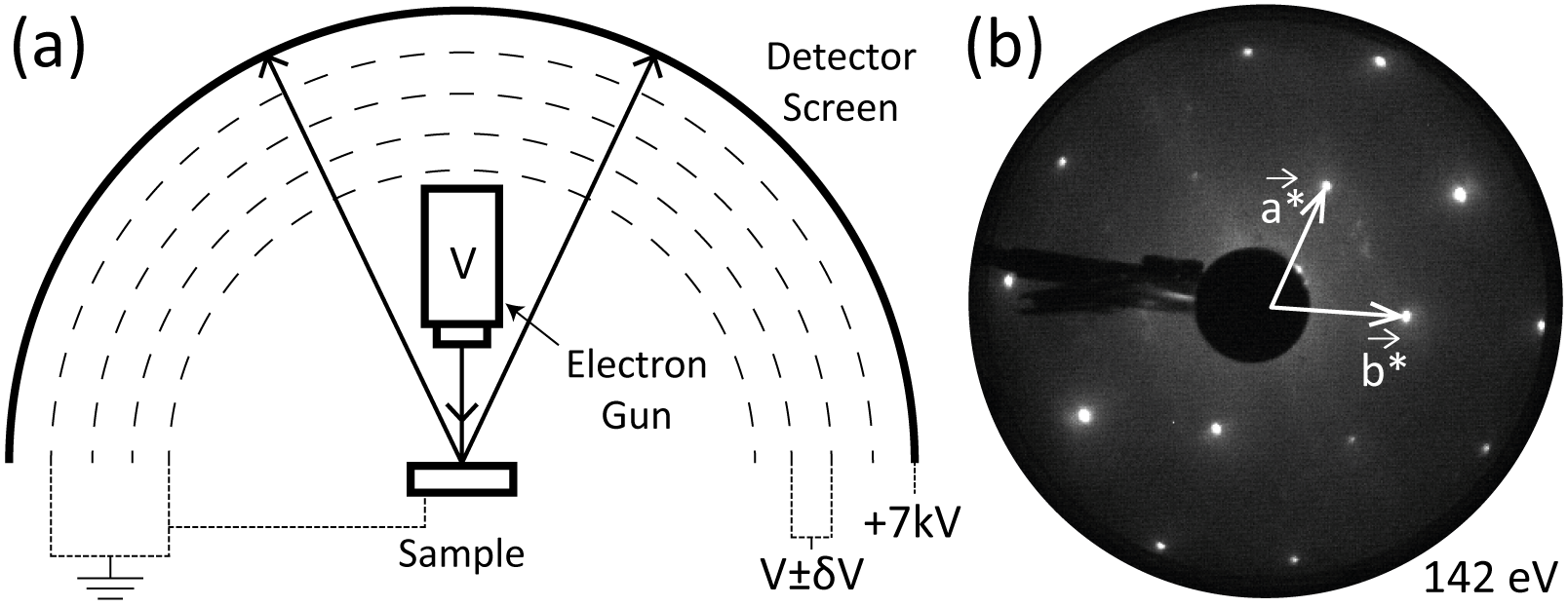
 and
and  are shown in white.