3.6 Charge transfer and rotation
As has been touched upon in previous sections, some molecules appear to switch
between “dim” and “bright” states [25, 35]. This phenomenon has previously
been attributed to C60-induced substrate reconstructions [25, 30–36]. Such
surface reconstructions lead to two topographically-different C60 adsorption sites,
where dim C60 molecules are sunk into nanopits on the reconstructed
substrate, and are lower in height than the bright ones [25, 30–36, 46]. The
switching between dim and bright C60 states was attributed to changes in the
substrate underneath the molecular layer due to the diffusion of substrate
atoms [25, 35]. Other explanations suggest that this apparent height difference
is due to electronic and molecular orientation effects [106, 107, 118].
Better understanding of the switching of C60 between different charge
states is central to further progress in electronic devices utilizing these
molecules.
This section describes the charge-transfer induced switching of some isolated
C60 molecules within the monolayer grown on the WO2/W(110) surface. Such
switching of individual C60 between different charge states represents a
phenomenon that is different from the “bright” and “dim” contrast shown in
Figure 3.10a, which was due to the “dim” molecules lying in the grooves between
the nanorows. Furthermore, these two phenomena coexist on the WO2/W(110)
surface. Our results indicate that C60 switching between charge states
correlates with the molecule’s rotation, i.e. some orientations of the molecule
favour its charge neutral state and others favour the negatively charged
state.
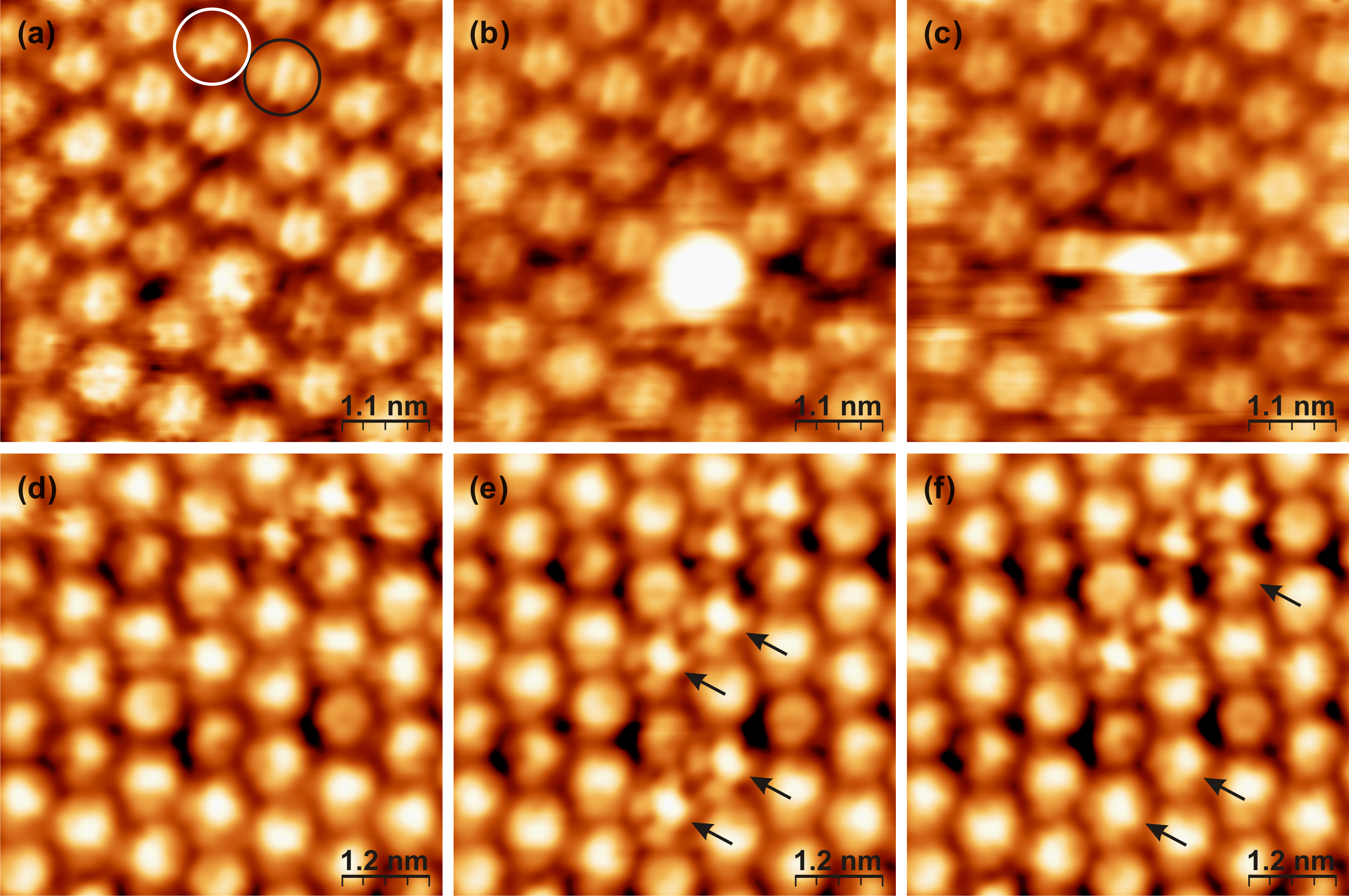
Figures 3.19a–c show a sequence of constant-current STM images of the same
area of the C60 monolayer self-assembled on the WO2/W(110) surface, acquired at
a sample bias of 1.0 V. These images, taken at 255 K, exhibit an internal structure
corresponding to molecular orbitals for most of the C60 molecules. Comparing
their appearance with the partial charge density calculated by DFT [46, 47]
(Section 3.5.3), it is noted that the majority of the molecules face the substrate
with an h–h bond (indicated by a black circle in Figure 3.19b), exhibiting three
distinct “stripes” [25, 31, 32, 46, 47, 161]. Most of the other molecules face the
substrate with an h–p bond (white circle). This is in agreement with DFT
calculations described in Section 3.5.3 which show that the h–h orientation has
the lowest total energy, while the h–p orientation differs from the lowest
energy state by 17 meV [47], which is comparable to kBT in our STM
experiments.
Although individual C60 molecules do not appear identical to one another
due to their different orientations on the surface [25, 30–36], the orbital
structure of each molecule remains unchanged from one image to the next,
indicating that these molecules are not rotating. However, some individual
molecules, such as the one at the centre of the image, switch between
different states. In the temperature range between the phase transitions
(220–260 K) such molecules change their appearance continuously in a
random fashion for the entire duration of the experiment. Figure 3.19c
demonstrates the case when switching occurs fast enough to be seen on a single
image. This phenomenon is observed at both positive and negative biases,
with the best apparent contrast achieved at a positive sample bias of
0.8 V.
Figures 3.19d–f show a sequence of constant-current STM images of another
area of the monolayer, acquired at a sample bias of -1.9 V. Several molecules are
observed to switch between scan frames (indicated by arrows). The apparent
height difference between the molecules in the two different states is much smaller
at this bias. The orientation of most of the molecules cannot be resolved at a
negative bias. However, the orbital structure of the molecules in the state which
has a lower apparent height is more pronounced and they are observed to be in
the h–p orientation on the surface. It is noted that imaging the surface with a
sample bias in the range of -0.5 V to 0.6 V, was unsuccessful, resulting
in noisy images. This was most likely due to the band gap of C60. At
lower temperatures the molecular switching between the different states
ceases and at high temperatures the molecules rotate continuously so
fast that no switching is observed and all molecules appear as perfect
spheres [47].
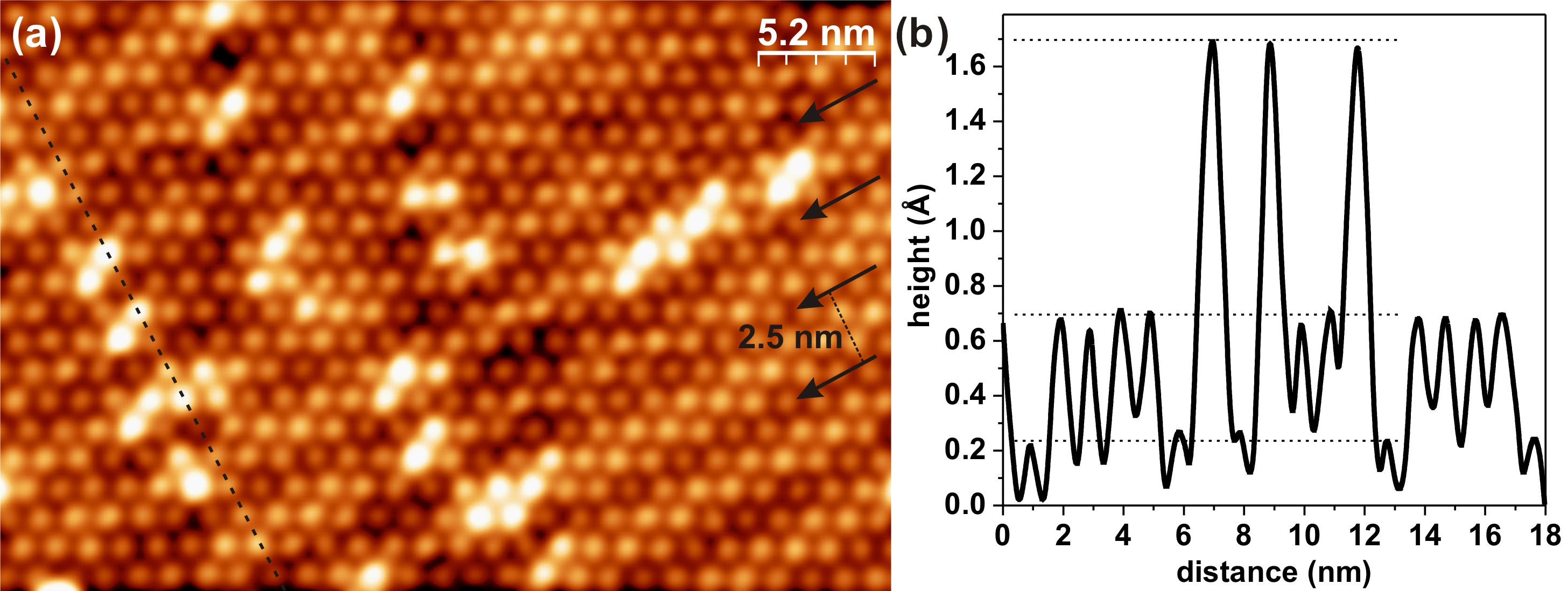
Figure 3.20a shows a constant-current STM image of the C60 monolayer,
acquired at 257 K. The image emphasizes the difference between the previously
described phenomenon of the “bright” and “dim” C60 contrast [25, 30–36] and
the C60 switching between charge states. Three types of molecules are
clearly visible in Figure 3.20a: “dim”, “normal” and “very bright”. They
are different in apparent height, which can be seen from the line profile
taken along the dashed line in Figure 3.20a and shown in Figure 3.20b.
The first two types represent “dim” and “bright” contrast due to the
substrate topography, with “dim” C60 molecules arranged in dark chain-like
structures on the surface (marked by the arrows in Figure 3.20). Such a
contrast is also observed at temperatures below 220 K as well as at both bias
polarities [46].
The distance between these chains is 2.5 nm, which is equal to the width of
oxide nanorows forming the substrate [46]. These “dim” C60 molecules follow the
oxide nanorows along the [337] direction of the substrate, occupy the grooves
between them, and, as a result, are situated slightly lower (by approximately
0.5 Å, see Figure 3.20b) than the “normal” C60. There are, however, very bright
molecules in Figures 3.19 and 3.20, with a much greater height difference of
about 1 Å (Figure 3.20b) between them and the “normal” C60. These very bright
molecules are predominantly located along the top of the oxide nanorows, with
very few of them found lying in the grooves between the rows, as can be seen in
Figure 3.20a.
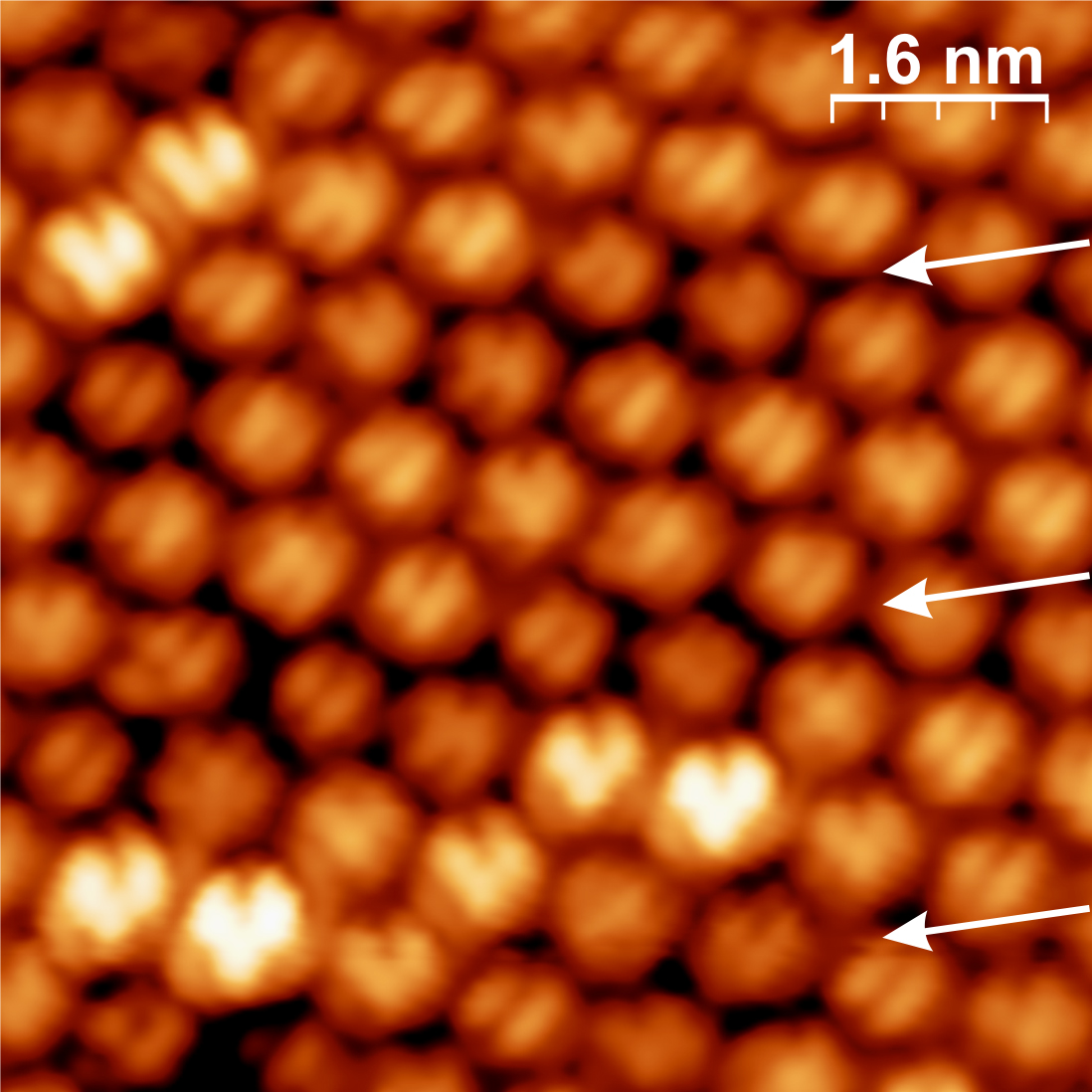
A majority of very bright molecules face the substrate surface with an h–p
bond, as can be seen in Figure 3.21. Furthermore, such C60 molecules change
their appearance in time, switching randomly between two different states.
The rate of switching between the states depends on temperature. In
the temperature range of 220–260 K, where switching is observed, the
total number of switching molecules rapidly decreases with decreasing
temperature.
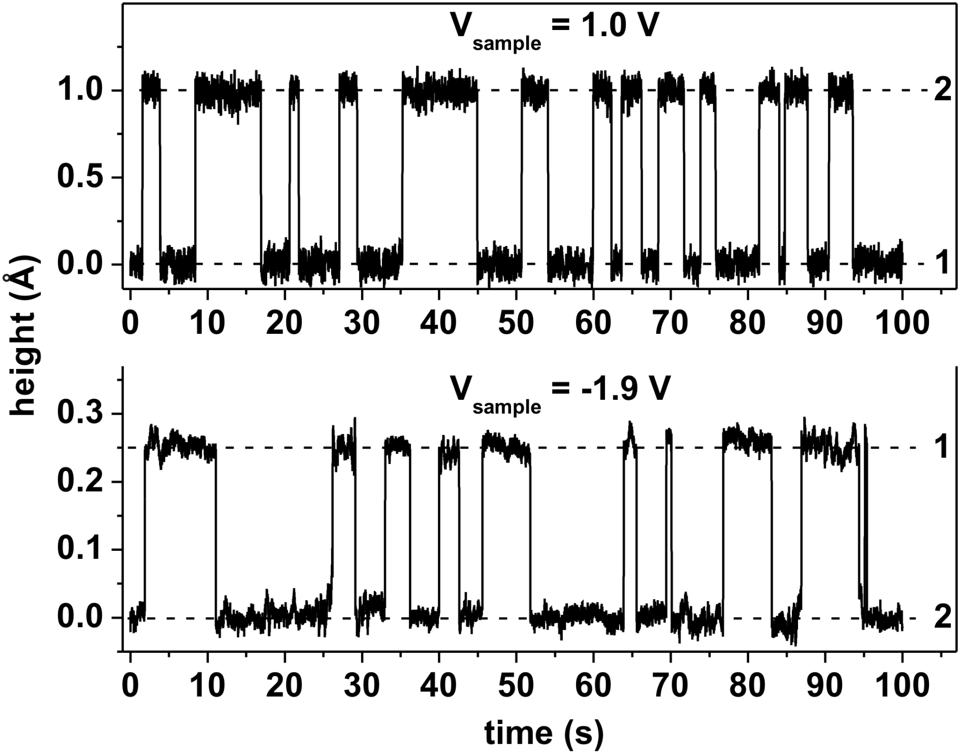
3.6.1 Switching time-evolution
The time-evolution of the tip-surface distance measured at two different sample
biases (1.0 V and -1.9 V) is presented in Figure 3.22, when the STM tip is placed
above an individual switching C60. In both cases the STM tip shifts between two
different height levels (indicated by dashed lines), corresponding to two different
states of the molecule. The tip-surface distance changes by approximately
1 Å during the switching of the molecule when a bias of 1.0 V is applied
(Figure 3.22, top spectrum). This cannot be explained in terms of different
geometrical orientations of the C60 on the surface or by C60-induced substrate
reconstructions [25, 30–36].
If, for example the C60 molecules were inducing the substrate to reconstruct,
the number of bright molecules would be conserved over time, as described by
Gardener and co-workers [25]. However in the present case, molecules are
observed to switch at random. The quality of the oxide substrate was confirmed
by STM prior to C60 deposition, and the film was found to have a very low
concentration of defects. Since C60 switching was observed over the entire sample
and was not limited to one particular area, it can be concluded that the effect is
not caused by the presence of defects.
It is suggested that this C60 state arises due to charging of the molecule, which
causes changes in the local density of electron states and consequently a variation
in tunneling current. Using density functional theory calculations, it was found
that the two different states of the C60 on the WO2/W(110) surface can be related
to: (1) the charge-neutral C60 (normal appearance, Figure 3.19a) and (2) the
negatively charged C60, which has accepted an electron (C−
60, very bright
appearance, Figure 3.19b). It is noted that, in most cases, switching between the
charge-neutral C60 in the h–h orientation and the C−
60 in the h–p orientation has
been observed (see Figures 3.19d–f).
However, in rare events, more than two states were distinguished during the
switching of some molecules, indicating that this phenomenon can be quite
complex. It is proposed that the negatively charged C60 state results from the
acceptance of a tunneling electron from the STM tip or the substrate depending
on the bias applied. This is based on the fact that the switching of the molecule
into the charged state is triggered continuously when the STM tip is static above
an individual C60 with a bias applied (as in Figure 3.22). Molecular movement
accompanies the molecule’s switching back to the charge neutral state, i.e., as
the molecule rotates, it loses charge to the substrate or neighbouring
molecules.
A similar charging process was observed by Repp et al., for the system of gold
atoms adsorbed on bi- and trilayers of NaCl grown on the Cu(111) and Cu(100)
surfaces [162]. By positioning the STM tip above an Au adatom and applying a
voltage pulse, the adatom can be reversibly switched between its neutral and
negatively-charged state. Both states have been found to be stable due to the
greatly suppressed mobility of Au adatoms at the temperature of the experiment
(5–60 K) as well as the reduced coupling of the electronic states of the adatom
with the metal substrate due to the insulating NaCl film [162]. Recently, it has
been shown that the charge state of molecules can be manipulated in a similar
manner [163].
STM experiments performed at temperatures below 10 K have revealed that
individual Cu phthalocyanine molecules deposited on the NaCl/Cu(111) surface
can be negatively charged by applying low voltage pulses [163]. In our
experiment, the ultrathin WO2 layer reduces the coupling of the electronic states
of the C60 with the W(110) substrate, which allows the molecule to hold
charge for some time. However, each C60 molecule that undergoes switching
is surrounded by six neighbours in the monolayer, resulting in van der
Waals interactions between the molecules. This interaction may influence
molecular movement and stability on the surface and hence affect the
switching.
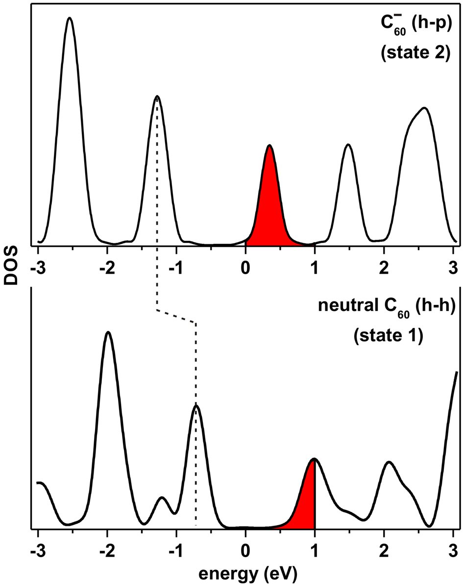
3.6.2 Density of states of C60
Figure 3.23 shows the density of states (DOS) calculated for two different
molecules, the charge-neutral C60 and the C−
60 with the h–h and h–p orientations,
respectively. The C60 orientation on the surface in each case has been chosen on
the basis of experimental observation that most of the “normal” molecules face
the substrate with an h–h bond, while the majority of very bright C60 face the
substrate with an h–p bond. The addition of an electron to the C60 molecule
changes its electron density of states. This results in the old lowest unoccupied
molecular orbital (MO) being half-occupied and becoming the new highest
occupied MO, which in turn causes the valence band structure to shift relative to
the Fermi energy.
The highlighted area in Figure 3.23 shows the molecular states involved in
tunneling, when a 1.0 V sample bias is applied. This bias leads to the apparent
height contrast of 1.0 Å between different molecular states in STM images (see
Figures 3.19 and 3.20) and corresponding changes in the STM tip-surface
distance (Figure 3.22, top curve). Note that there is a significant increase in the
molecular states available for tunneling (in the energy range from 0–1.0 eV) in
going from the charge-neutral C60 molecule (state 1) to the C−
60 (state 2), which is
reflected in the very bright appearance of the latter at the 1.0 V sample
bias.
A difference in DOS for the C−
60 and C60 molecules (Figure 3.23) suggests
that the apparent height difference ΔZ should depend on the applied
bias voltage. Indeed, at sample biases higher than 1.5 V (or lower than
-1.5 V), the observed apparent contrast between different C60 states was
significantly smaller because multiple molecular orbitals were involved in
tunneling. This minimizes the difference between the DOS for each state of
the C60 characterised by the molecule’s charge and orientation on the
surface.
From Heisenberg’s uncertainty principle, ΔEΔt > ℏ∕2, the energy resolution
of a state should be inversely proportional to its lifetime [164], i.e. an electron
should only exist for a short time in a state whose energy range is broad. This
would imply that the broad states calculated in Figure 3.23 should only lead to
an observed lifetime on the order of femtoseconds, however one must
remember that for the system in question, charge transfer is not the only
phenomenon that must be accounted for. In going from the neutral C60 to
charged C−
60, the molecule must rotate from h–h to h–p, which will have its
own associated characteristic timescale, and the presence of the STM
tip causes charging to be constantly triggered by tunneling electrons.
The tip itself may also affect the rotation of the molecule, thus the full
complexities of the switching mechanism are not encompassed by simply
calculating the DOS for the two “final” states, however it is illustrative in
explaining the apparent contrast between the two observed states. It is
unfortunately beyond the scope of this thesis to develop a full theoretical basis for
the switching mechanism, however it is an interesting avenue for future
work.
The STM tip-surface distance changes by only 0.25 Å during the switching of
the molecule with -1.9 V bias applied (Figure 3.22, bottom curve). This is due to
the relatively small difference between the molecular states of C60 and C−
60
available for tunneling between -1.9 eV to 0 eV. At this bias the C−
60
molecule (state 2) has a slightly darker appearance in STM images than the
charge neutral C60 (Figures 3.19d-f), which is in good agreement with the
STM tip-surface distance obtained at -1.9 V bias (Figure 3.22, bottom
curve).
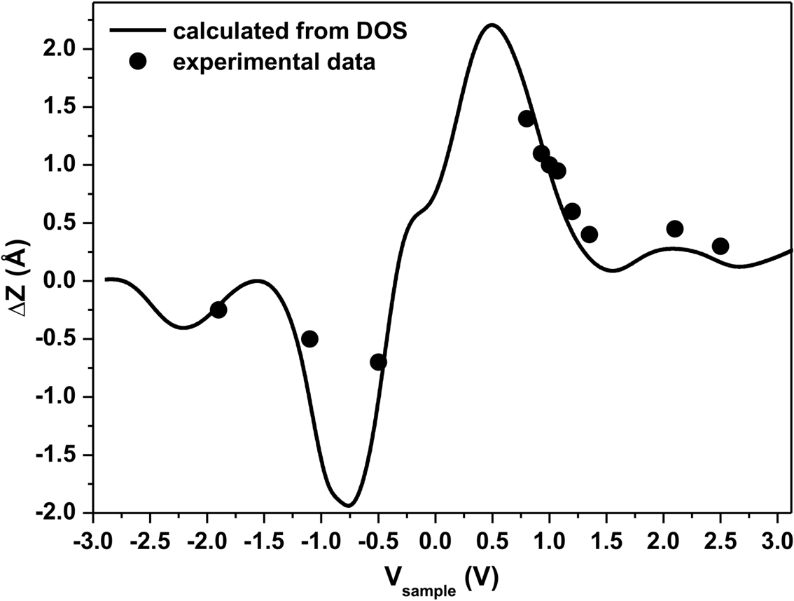
In constant current mode, the apparent height difference ΔZ between the C−
60
and the C60 molecules can be determined as:
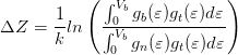 | (3.1) |
where gb(ε) and gn(ε) are the DOS of the C−
60 and C60, respectively, gt(ε) is the
DOS of the STM tip and k = 2Å -1 [165]. The DOS of the monocrystalline
W(100) tip, previously calculated in this group [74, 166], exhibits no major
features close to the Fermi energy and can be treated as nearly constant in the
range considered here. Although it cannot be guaranteed that the tip does not
have an attached molecule during the experiments, STM performed before and
after z(t) measurements were consistent with the most stably-observed
appearance of the film, and so it is assumed for simplicity that the tip apex
consists of only clean tungsten.
Using this formula, the ΔZ between the C−
60 (h–p orientation) and the C60
(h–h orientation) molecules on the WO2/W(110) surface has been calculated from
the density of states presented in Figure 3.23 under the assumption that gt(ε) is
nearly constant and is shown in Figure 3.24 as a solid line. This curve is in good
agreement with the experimental data for ΔZ obtained from STM images and the
time-evolution of the tip-surface distance measured at different sample biases. The
data presented in Figure 3.24 indicate that both a large value of ΔZ at
certain biases and its overall dependence on bias voltage can only be
explained in terms of different charge states of the C60 molecules on the
surface.
These observations are in good agreement with the results of Yamachika et al.,
obtained during their low-temperature study of controllable C60 doping with K
atoms on the Ag(001) surface [167]. They have found that approximately 0.6 of
an electron is transferred to C60 from each K. They have observed only small
changes in apparent size between the C60 and K4C60 molecules when scanned at
2.0 V sample bias. At this bias the number of orbitals involved in tunneling does
not change dramatically when going from C60 to K4C60, as observed by scanning
tunneling spectroscopy [167]. However, the  map measured at 1.25 V and 50 pA
was found to be much brighter in the case of the K4C60 molecule, where
approximately 2.4 electrons are transferred to the C60, than in the case of
undoped C60 [167].
map measured at 1.25 V and 50 pA
was found to be much brighter in the case of the K4C60 molecule, where
approximately 2.4 electrons are transferred to the C60, than in the case of
undoped C60 [167].
3.6.3 The Fukui function of charge states
It has been observed that switching C60 molecules change their orientation on the
surface. Furthermore, most of the “normal” molecules face the substrate with an
h–h bond, while the majority of negatively charged C60 face the substrate with an
h–p bond. It is reasonable to propose that the process of gaining or losing an
electron depends on the C60 orientation. Charge transfer efficiency to or from the
molecule depends strongly on which part of the molecule is most reactive.
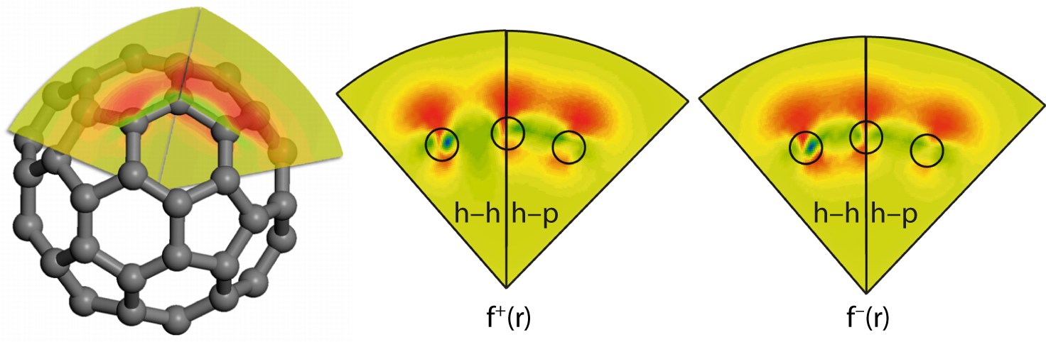
The spatially-resolved reactivity of the molecule can be visualized by
the Fukui function, f(r), which is considered as a convoluted reactivity
indicator [168].
The Fukui function (f+(r) or f−(r)) is defined as the differential change in the
electron density due to an infinitesimal change (increase or decrease) in the
number of electrons. When the molecule accepts electrons, the electrons tend to
go to the part of the molecule where the Fukui function f+(r) is large, because
at these locations the molecule is most capable of stabilizing additional
electrons [168].
Figure 3.25 shows cross sections of f+(r) and f−(r) taken along the h–h and
h–p bonds through the centre of the C60, calculated using Dmol3 (Accelrys
Materials Studio 4.3). The value of f+(r) (centre panel) is larger for the h–p bond
with respect to the h–h bond, in agreement with previous calculations [168]. This
indicates that the addition of electrons to C60 is more effective when an h–p bond
of the molecule faces the WO2/W(110) surface and, due to the molecule’s
symmetry, the STM tip.
In turn, the analysis of f−(r) (Figure 3.25) allows one to conclude that the
removal of an electron occurs more effectively via h–h bonds. Thus a strong
correlation between the charge state of the C60 molecule and its orientation on the
surface observed in experiments can be explained in terms of charge transfer
efficiency. Electron acceptance by the molecule is facilitated through its rotation
to achieve an h–p orientation, which is the most suitable for such charge transfer.
In turn, electron loss is accompanied by the molecule’s rotation back to an h–h
orientation.
Combining all the findings, the following mechanism for the C60 switching on
the WO2/W(110) surface can be proposed. When the molecule in the neutral
state is facing the surface by an h–h bond, there are four h–p bonds in the lower
(or upper) part of C60 which are located in a symmetric way around this h–h
bond. Due to thermal excitation of the molecule, one of these h–p bonds may
come closer to the surface (or the STM tip) than the other three and accept an
electron. This leaves the negatively charged molecule locked to the surface
via this h–p bond. The ultrathin WO2 layer reduces the coupling of the
electronic states of the C60 to the W(110) substrate, which allows the
molecule to hold this charge for some time. However, each C60 molecule that
undergoes switching is surrounded by six neighbours in the monolayer,
resulting in van der Waals interactions between them. This interaction may
influence molecular movement and trigger the loss of the electron. This
view is simplified to highlight the correlation between the charging of C60
and its movement on the WO2/W(110) surface. There can be additional
complexities one may need to take into account. For example, our calculation of
the Fukui function was done for an isolated C60. The proximity of the
molecule to the WO2/W(110) surface and to an STM tip will alter the Fukui
function.