3.4 Growth and topography of the C60 film
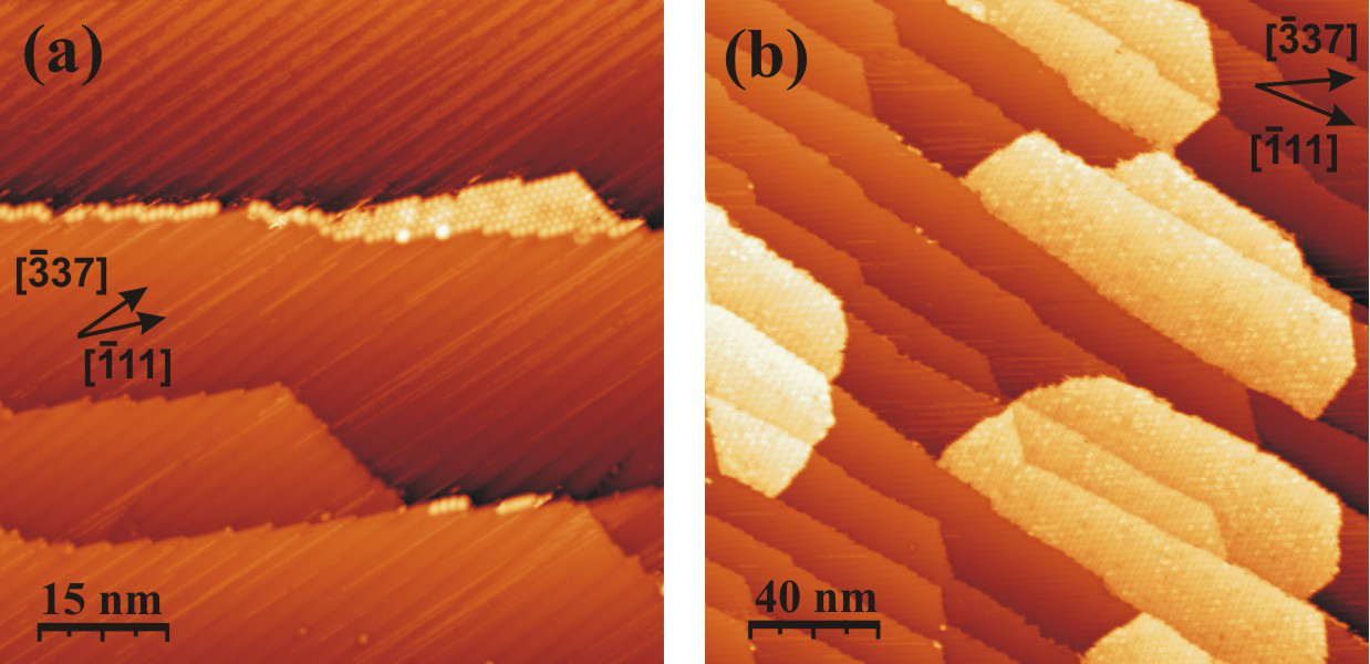
At a very low coverage (0.2 ML), C60 molecules start nucleating at the inner step
edges of the WO2/W(110) surface (see Figure 3.8a), which provides evidence for a
weak molecule-substrate interaction and for the diffusion of the molecules on the
surface at room temperature. C60 molecules appear as bright protrusions in the
STM images and decorate the substrate’s inner step edges, forming molecular
chains. The tungsten oxide nanorows of the underlying substrate are also visible
(Figure 3.8a).
At intermediate coverages (0.4–0.7 ML), C60 molecules self-assemble at room
temperature into compact two-dimensional islands with a hexagonal close packed
structure (see Figure 3.8b). The C60 molecular layer is incommensurate with the
WO2/W(110) substrate. However, the growth of the C60 overlayer starts from the
substrate’s inner step edges, which follow the [111] direction on the surface. This
behaviour causes one of the primary directions of the molecular layer to
coincide with the [111] direction of the WO2/W(110) surface. This is a
clear indication that the substrate plays a certain role in the adsorption
and arrangement of the molecules. The angle between this direction of
the C60 layer and the [337] direction of the oxide nanorows is equal to
23°.
The intermolecular bonding that occurs through the C60 π-electron system
appears to be stronger than the molecule-substrate interaction, leading to the
formation of such compact islands. This is confirmed by the fact that there are no
single C60 molecules adsorbed in the middle of substrate terraces after deposition,
indicating a high mobility of the individual molecules on the surface at room
temperature. Furthermore, each WO2/W(110) substrate terrace is covered with a
single molecular domain, with terrace widths of up to 40 nm, and domain
boundaries are rarely observed. The distribution of the C60 among the
substrate terraces is not homogeneous at this coverage – some terraces
have almost no C60. This indicates that C60 molecules can easily cross
substrate step edges while moving on the surface as a result of inter-terrace
diffusion.
At approximately 1 ML coverage, the molecules form large domains whose
width is limited only by the width of the WO2/W(110) substrate terraces. One
molecular monolayer is defined as the case in which the substrate is completely
covered by molecules such that if one further molecule is added, it will have no
direct contact with the substrate and will form a second layer. For the C60
monolayer on the WO2/W(110) surface, the molecular packing density is 1.25 C60
molecules per 1 nm2.
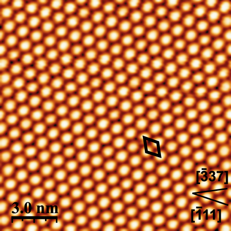
The unit cell of the C60 lattice (shown in black in Figure 3.9) contains a single
C60 molecule and its unit cell vectors are each equal to 0.95 ± 0.05 nm, with an
angle between them of 60.0 ± 0.5°, forming a hexagonal close-packed structure.
The intermolecular separation within the overlayer is very close to the natural
molecule-molecule distance of 1 nm observed in bulk C60 crystals. The formation
of ordered domains of such an extent and the C60–C60 separation further indicate
the presence of a significant intermolecular interaction, as well as a low
diffusion barrier for the molecules on the WO2/W(110) surface at room
temperature. Thus, C60 molecules are physisorbed on this surface and a weak
molecule-substrate interaction occurs through the molecular π-electron
system.
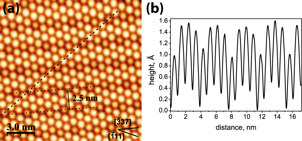
At some voltage biases, the C60 molecules on the WO2/W(110) surface show a
significant difference in apparent height (see Figure 3.10a), which can be a
reflection of local electronic and/or topographic variations.
These so called ‘bright’ and ‘dim’ molecules have been previously observed by
STM on a variety of surfaces and are often attributed to C60-induced substrate
reconstructions [25, 30–37]. Such surface reconstructions can lead to two
topographically different C60 adsorption sites, where ‘dim’ C60 molecules are sunk
into nanopits of the reconstructed substrate, and are lower in height than ‘bright’
ones. Other explanations suggest that this apparent height difference is due to
electronic and molecular orientation effects [106, 118]. From Figure 3.10a it is
clearly seen that the ‘dim’ C60 molecules on the WO2/W(110) are arranged in
dark chain-like structures. The distance between these chains is equal to 2.5 nm as
observed by STM.
From STM images it is clear that the ‘dim’ C60 molecules follow the oxide
nanorows of the substrate and are adsorbed between them. The nanostructured
WO2/W(110) surface exhibits grooves separated by 2.5 nm [94], which are seen as
dark depressions in the STM image (Figure 3.6a). The ‘dim’ C60 molecules
observed in Figure 3.10a occupy these grooves, and are situated slightly lower
than the others (‘bright’ C60). The line profile shown in Figure 3.10b indicates
that the height difference between the ‘bright’ and ‘dim’ C60 molecules is equal to
approximately 0.6 Å. The same value of corrugation was observed for oxide
nanorows forming the WO2/W(110) surface [94], indicating that such an
apparent height difference between C60 molecules is due to the substrate
topography.
Furthermore, a similar apparent height difference in the range of 0.4–1.0 Å,
attributed to an adsorbate-induced reconstruction of the substrate,
has been observed between ‘bright’ and ‘dim’ C60 molecules on other
surfaces and was explained by an adsorbate-induced reconstruction of
the substrate [25, 30, 33–35]. However, there is also the possibility of
a slightly different interaction between the WO2/W(110) surface and
the electron orbitals of the ‘dim’ C60 molecules, caused by their specific
arrangement on the surface, which results in proximity of the molecule to the W
layer.
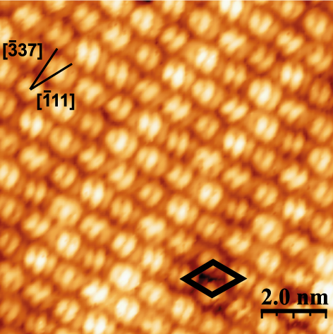
Low-temperature STM of C60 molecules performed at 78 K demonstrates
well-resolved molecular orbitals within individual molecules. It was not possible to
resolve these orbitals by performing STM at room temperature. This
is due to movement (rotation) of the molecules within the layer at this
temperature, and will be discussed further in the following Sections 3.5 and
3.6.
At 78 K however, most of the molecules in the complete C60 monolayer on the
WO2/W(110) surface exhibit the same internal stucture, and are rotated
approximately in the same direction due to interactions with the substrate and
the suppression of molecular movement at such a low temperature. This is shown
in Figure 3.11 by the ordered molecular orbitals (lobes) of individual C60. The
molecules appear on the STM image as spheres composed of three ‘stripes’
(molecular lobes), suggesting that the same part of each C60 molecule is
facing the substrate. The similar appearance of most of the C60 on the
WO2/W(110) surface indicates that the molecule-substrate interaction is strong
enough to align the molecules at low temperature, when their movement is
suppressed.
Similar parallel orientation of C60 molecules has been previously observed on
certain other surfaces by low-temperature STM [28, 30, 33, 34, 89]. It is noted
that STM images exhibiting three molecular lobes within an individual C60
molecule have been acquired at a sample bias in the range from 0.7–1.0 V
(0.9 V in Figure 3.11). At such a voltage, electron tunneling occurs into
the lowest unoccupied molecular orbital (LUMO) of C60, making the
LUMO responsible for the ‘three-stripe’ appearance of C60 molecules on
the WO2/W(110) surface. C60 molecules exhibiting three ‘stripes’ have
been previously observed by STM on different metal and semiconductor
surfaces [25, 31, 32, 41, 119, 120]. In most of these cases the proposed C60
orientation was the one in which the carbon-carbon bond that forms the
border between two adjacent hexagons of C60 (h–h bond) is parallel to the
substrate [31, 32, 41, 119, 120].