“herringbone” reconstruction underneath
the C60 layer, however these two isolated regions are all that remain of the original
22 ×
“herringbone” reconstruction underneath
the C60 layer, however these two isolated regions are all that remain of the original
22 × structure, indicating that the C60 layer has lifted the reconstruction over
the majority of the surface.
structure, indicating that the C60 layer has lifted the reconstruction over
the majority of the surface.
The fabrication of complex organic molecular structures on technologically important substrates held together by weak and reversible van der Waals interactions, hydrogen bonds or electrostatic interactions has been a much-investigated topic in the past ten years [9–11, 76–82]. This controlled self-assembly of organic nanostructures offers a number of powerful approaches for the development of organic molecule-based devices, which possess functions such as rectifying, switching and sensing [10, 11, 15, 76–81, 83, 84].
Fullerenes in particular have attracted considerable attention in recent years due to their potential in surface chemistry and nanotemplating [84], non-linear optics [84, 85], single-molecule transistors [15, 20], and especially molecular electronics because of their tuneable electronic properties, resulting in superconducting or semiconducting behaviour [15, 86, 87].
The formation and characterisation of fullerene adlayers on surfaces are of great interest from the fundamental and technological points of view because they provide valuable information about molecular interactions and can lead to potential applications in existing technologies.
The study of these surface-supported systems is important for future developments in molecular electronics, since they represent promising materials for applications in advanced nanopatterning, surface templating, molecular data storage, solar cells, sensors/molecular recognition and functional surfaces [14, 15, 20, 22, 84–88].
Of particular interest are the nature of the bonding between the fullerene molecules and the substrate, as reflected in the electronic charge distribution and their geometric configuration at the interface, and the dynamics of electron-hole transfer between the molecule and the metal or semiconductor surface. This information can be obtained by using a combination of scanning tunneling microscopy and theory (STM and DFT).
STM is a highly local technique that has become a powerful tool for studying the adsorption geometry and the conformation and dynamics of single organic molecules and molecular assemblies on conducting substrates [9–11, 76–82]. Over the last decade STM has been used intensively for the study of C60 self-assembled layers on a variety of metal [18, 24–37] and semiconductor [22, 38–42] surfaces.
On most surfaces fullerene molecules self-assemble into close-packed monolayers with a hexagonal or quasi-hexagonal structure and a molecule-molecule separation close to 1 nm, as observed in bulk C60 [18, 22, 24–27, 29–39, 42, 89]. In some cases the formation of a C60 monolayer leads to an adsorbate-induced reconstruction of the substrate [25, 30–37].
Surprisingly, only few studies of C60 on metal oxide surfaces have been performed to this end [43–45]. This is despite the fact that metal oxide surfaces and thin films have many potential applications in existing technologies [90–93] and may be used as nanostructured templates with preformed surface patterns [94–97] for molecular self-assembly.
The choice to study the combination of C60 and WO2/W(110) in this work was motivated in part by the expertise present in the research group. Dr Kevin Radican had recently described the WO2/W(110) surface in detail [94], and the width of the oxide nanorows (∼2.5 nm) was expected to lead to some interesting templating behaviour of adsorbates. Similarly, Dr Sergey Krasnikov joined the group and brought with him vast experience on molecular self assembly, and so C60 was chosen as a test molecule about which a large amount was known from the literature. It was expected that C60’s dynamic behaviour could be explored by controlling the temperature, which could give insights into fundamental physical processes.
C60 has been well studied on many metal surfaces, and some common properties and differences can be derived from past research. Arguably the most studied C60/metal system is C60 on Cu(111) [37, 98–102]. The Cu(111) lattice and that of solid C60 have only a small 2% lattice mismatch, making the substrate ideal for the growth of films. Detailed theoretical calculations show that the most stable adsorption site on Cu(111) is the so-called “hcp” hollow site, with the hexagon facing down (h-orientation, see below) [99, 100]. However the hcp (h-orientation), fcc (p-orientation, pentagon facing down) and bridge (h or p) sites of the close-packed surface are very close in energy, leading to a very high C60 mobility when the molecules have rotational and translational motion [98]. This leads to a hexagonal close-packed monolayer formed on the surface [101, 102].
Upon the formation of a monolayer, the Cu surface is reconstructed, with the Cu–Cu bonds closest to the C60’s bottom hexagon elongating and forming a nanopit. In turn the short and long C–C bonds of the bottom hexagon extend by 3% and 2%, respectively [98]. This assembly is accompanied by a charge transfer of 1.5–2 electrons/C60 from the surface to the molecules as measured by NEXAFS [103, 104].
Interestingly, when a monolayer of C60 is deposited on a thin layer of Cu, the sheet resistance of the system is decreased, however when deposited on a thick Cu layer, its sheet resistance is increased [105]. The explanation for this is that the thick Cu is a good conductor, and the presence of the molecule/metal interface introduced extra scattering processes, causing the conductance to suffer.
Gardener et al. have studied the dynamics of a monolayer of C60 on the noble
Au(111) surface [25]. They observed that some molecules appeared darker than
others in the monolayer, and the amount of dark molecules appeared to be
correlated to the registry of the overlayer with the substrate. Figure 3.1a shows a
characteristic image of a quasi-periodic domain. The two bright features
highlighted by arrows show the 22 × “herringbone” reconstruction underneath
the C60 layer, however these two isolated regions are all that remain of the original
22 × structure, indicating that the C60 layer has lifted the reconstruction over
the majority of the surface.
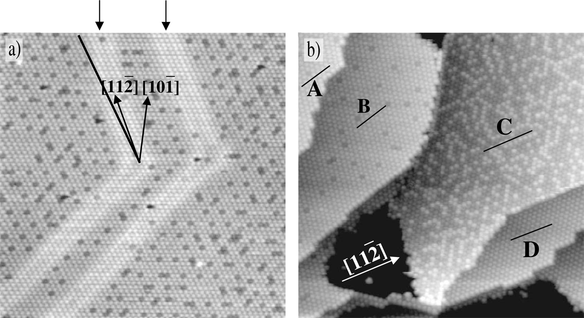
Figure 3.1b illustrates several different domains A−D within a post-annealed C60 monolayer on the Au(111) surface. These domains are characterised by the arrangement of “dim” C60 molecules which have a lower apparent height than other C60. D shows a domain with a uniform apparent height, whereas domains A and B exhibit the so-called quasi-periodic structure of dim C60 molecules, and C demonstrates a disordered structure.
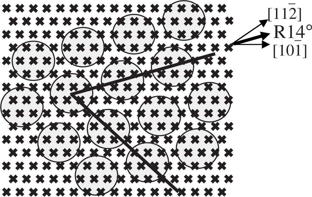
The fundamental difference between these domains is the angle made between the primary directions of the C60 overlayer and the crystallographic directions of the substrate, as indicated by solid black lines in Figure 3.1b. C and D are aligned along the [11] direction of the Au(111) surface, implying a strong correlation between the uniform and disordered regions of the monolayer, whereas A and B are offset by an angle of 16° from this direction. This is indicative of a 7 × 7 R14° superstructure for these domains, as shown in Figure 3.2, where every seventh C60 molecule occupies the same Au lattice site, giving rise to the quasi-periodicity observed in A and B.
The apparent height differences between individual molecules in each domain exhibit a dynamic behaviour, with many molecules switching between high, medium and low states. This switching has been attributed to charge transfer occurring between the C60 molecules and the Au substrate, with such transfer accommodated by nanopits forming via substrate reconstruction.
Early work on C60 adsorption on Ag(111) disagreed on its binding and absorption sites, with the group of Eric Altman proposing the p-orientation C60 on the on-top site [106, 107], and Takayasu Sakurai showing the favoured adsorption as the h-orientation on the hollow site [101]. Time has borne out the latter interpretation, with numerous theoretical [98] and experimental works [108–110] and confirming that the hollow site model has the lowest energy, however with some dynamical behaviour observed by STM [108].
Similar to the case on Au(111), C60 causes the Ag(111) surface reconstruction to change position over time [108–110]. This is represented as an apparent contrast between some C60. Such contrast is observed to switch over time in a correlated fashion at room temperature. This behaviour is explained by the mass transport of Ag atoms along the surface, i.e. at one point C60 will be sitting on-top of a Ag atom, and during the next scan the surface atoms have shifted and it will be sitting in a hollow site. Although the hollow site has the lowest energy, the on-top site with the hexagon-hexagon C–C bond (h–h) facing the substrate is only slightly higher in energy, and from the temperature dependence of the switching rate, an energy barrier of 0.84 eV has been derived between the two states [108].
This dynamical behaviour on noble metal surfaces is well-understood and indeed a recent study asserted that it appears that “interface reconstruction of close-packed metal surfaces induced by large-molecule C60 adsorption is the rule rather than the exception” [110], however as will be shown in Section 3.6, the results on WO2/W(110) do not support substrate reconstruction, instead the ultrathin O–W–O trilayer decouples the C60 organic layer from the metallic substrate, allowing the charge-states to have a finite lifetime without the need for surface reconstruction.
In contrast to the high-mobility, van der Waals-bound systems discussed so far, when deposited on Pt(111), C60 is very strongly bound and immobile [111]. At room temperature (300 K), the Pt surface catalyses the polymerisation of the C60, and at higher temperatures (∼1050 K) the molecules decompose [112]. Similarly on Pt(110), there is a strong interaction with the surface, with C60 lifting the so-called “missing-row” reconstruction, and forming a dumbbell-shaped nanowire array above 700 K [113]. Decomposition is also observed on Ni(110) with a carbon layer formed at about 760 K, transforming into graphitic carbon at higher temperatures [37, 111, 114].
On semiconductor surfaces the molecules can be even more strongly bound, however studies of C60 on Si(001)-(2 × 1) and Si(111)-(7 × 7) show only physisorption until the systems are annealed up to 670 K, at which temperatures strong covalent bonds are formed [115–117]. Decomposition to SiC is observed when the temperature is increased above 1000 K.
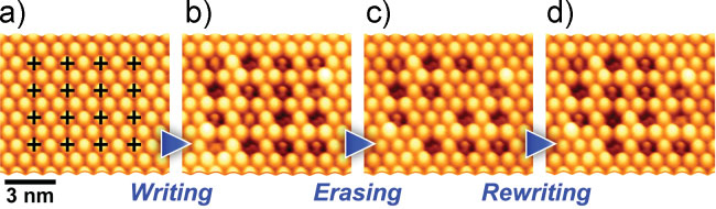
Nakaya et al. [22] have demonstrated data storage on the molecular scale
using a trilayer of C60 molecules prepared on the passivated Ag/Si(111)- ×
× R30° substrate. By controlling the bias voltage of the STM tip, it was shown that
the C60 in the overlayers could be induced to form dimer and trimer structures,
which were visible as dark depressions in the formerly pristine close-packed
structure of the film (Figure 3.3).
R30° substrate. By controlling the bias voltage of the STM tip, it was shown that
the C60 in the overlayers could be induced to form dimer and trimer structures,
which were visible as dark depressions in the formerly pristine close-packed
structure of the film (Figure 3.3).
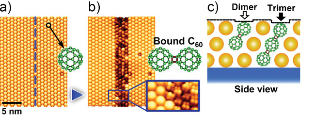
 ×
× R30°. (b) After
scanning the tip along the dotted line at 60 nm s-1 with a sample bias of
-3.5 V, a dark line of bound C60 is formed. (c) Schematic of dimer and trimer
formation [22].
R30°. (b) After
scanning the tip along the dotted line at 60 nm s-1 with a sample bias of
-3.5 V, a dark line of bound C60 is formed. (c) Schematic of dimer and trimer
formation [22].
It was also shown that the induced depressions could be repaired by pulsing with a bias voltage of opposite polarity, and the process could be repeated multiple times with no adverse effects on the C60 molecules (Figure 3.4).
Finally, the few studies of C60 on metal oxides thus far have focussed on either SrTiO2 [43] or TiO2 [44, 45]. On TiO2(110), C60 grows in an island fashion, with each C60 bridging a groove between two oxygen rows [44]. Although the rutile TiO2 surface is inherently defective, the C60 overlayer is quite free of defects, indicating a stronger molecule–molecule interaction than the molecule–substrate interaction, with images of isolated molecules very rare.
In summary, C60 has been widely studied on a range of metal, semiconductor and metal oxide surfaces, several of which show an apparent contrast between some molecules, attributed to either surface reconstruction or molecular polymerisation, however it will be shown in the following sections that the contrast observed on WO2/W(110) cannot be attributed to either of these explanations, and instead is due to charge transfer to the C60 molecules.
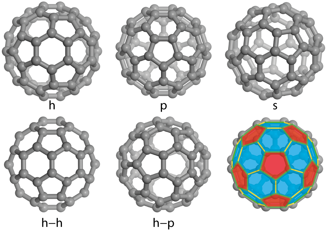
Although C60 is a spherical molecule, it is not completely symmetric, in that it has discrete faces, bonds and atoms, and so when it is deposited onto a surface, five different high-symmetry orientations are possible, as shown in Figure 3.5. When the 6 or 5 atoms in either a hexagonal or pentagonal face of the molecule is directed towards the surface, that orientation will be designated h or p, respectively. Similarly two atoms can form either the border between two hexagons (h–h) or a hexagon and a pentagon (h–p). Finally, each of the C60’s 60 carbon atoms are identical, so if the molecule faces the surface by a single atom it is designated s. The final panel in Figure 3.5 shows the relationship between the faces and bonds in one half of the C60 molecule.